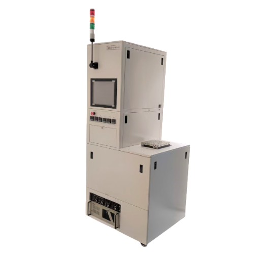
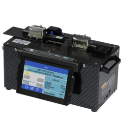
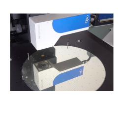
ALD System
Category: Electronic Production Manufacturing Equipment
Exhibitor: DAH YOUNG VACUUM EQUIPMENT CO., LTD.
Booth No: N328
Characteristic
Atomic Layer Deposition (ALD) is a new process that can be used to replace chemical vapor deposition (CVD), plasma-assisted chemical vapor deposition (PECVD), and sputtering technologies. Atomic layer deposition is also a type of chemical vapor deposition (CVD) technology. The difference from CVD is that ALD divides the traditional CVD reaction process into two half-reactions. One is the Chemisorption saturation process of the precursors, and the other is the Sequential surface chemical reaction process.
The precursor product and the material surface undergo a continuous, self-limiting (Self-limiting) reaction. The material is slowly deposited by reacting with different precursor products separately, and the substance is plated on the surface of the substrate in the form of a single atomic layer. The deposition of a material at (1 ~ 2 Å), so the growth of ALD material is controlled in the thickness range of a single atomic layer, forming a step coverage and large area uniformity.
Atomic layer deposition has the characteristics of high density, high thickness uniformity, high step coverage, low temperature process and atomic-level precise thickness control. In addition to ultra-thin and high-dielectric material coating, it can also target tiny circuit structures. Provide hole filling ability, such as the structure with high aspect ratio and related areas to provide a uniform thickness coating. Atomic layer deposition is a key semiconductor device assembly method, and it can also become a future development area in some nano material synthesis methods, including semiconductor integrated circuits, micro-electromechanical, thin-film transistors, OLED displays and component packaging.
Other Products
Products you may be interested in
-
High Rigidity of Hydrostatic Cylindrical Plunge Grinding Machine
-
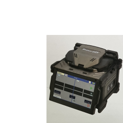
Fujikura CT-115/116
-
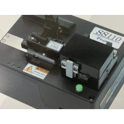
Laser Modification machine
-
Ultrasonic Cleaning Basket
-

Fujikura Optical Recoater FSR-115/116/117
-
Miniature Spectrometer
-
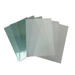
Functional Coating Films
-
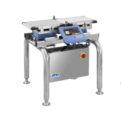
Check Weigher
-
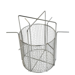
Ultrasonic Cleaning Basket
-
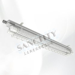
Explosion-proof Fluorescent Lamp with Ex d Rating
-
OGP SNAP350 Large Field Of View Video Measuring System
-
Automated thin film thickness measure and analysis system
-
High Temperature Resistance Brush
-
Three-Temperature Separation Technology
-
Fujikura 45S fusion splicer
-
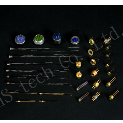
Al6061/Cu1100/Ti Headers
-
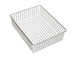
Cleaning Basket
-
Fujikura光纖熔接機
-
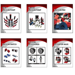
VACUUM PUMP/ACCESSOREIS/SWITCH
-
Microelectronic Packaging
-
ULTRA PURE WATER GENERATION EQUIPMENT
-
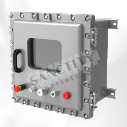
Explosion-proof Human-Machine with Ex d tb Rating
-
OGP E7 Fully Automatic Measurement System
-
Large capacity syringe filling machine
-
G-Series side channel blowers
Highest Rated Products
-
Printing Equipment for Display Industry
-
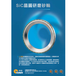
Wafer Grinding Wheels for Silicon Carbide
-
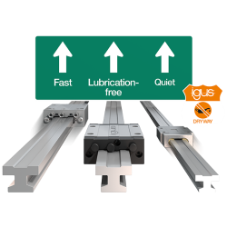
igus linear system
-
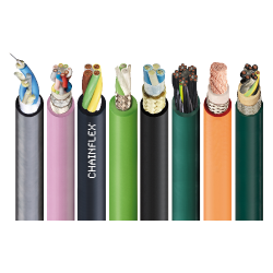
chainflex® cables
-
Low-cost automation
-
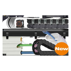
e-chains system
-
Steering Mirror
-
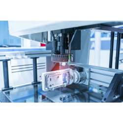
Automated Motion Control
-
Focus tunable lenses
-
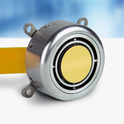
Imaging Modules
-
3D optical microprofilometer(white light interferometer)
-
Absolute Position Measurement System
-
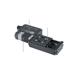
SSA Single Axis Linear Motor Stage
-
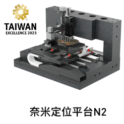
Nano-positioning stage N2
-
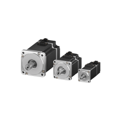
E Series Servo Motor
-
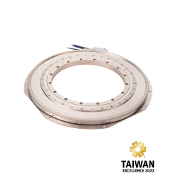
DMT Series Ultra-thin Direct Drive Motor
-
VIDEO PATTERN GENERATOR
-
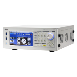
FPD TESTER
-
SMALL SIZE MEASURING PROBE
-
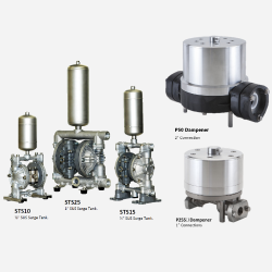
Liquid/Surge Tank Pulsation Dampeners
-
D200 D250 Series
-
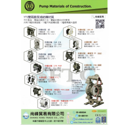
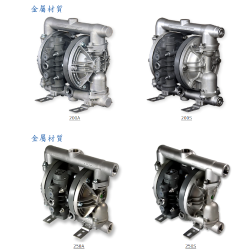
YTS Pump Materials of Construction
-
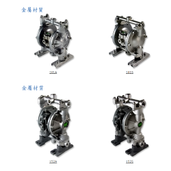
D101 D152 series
-
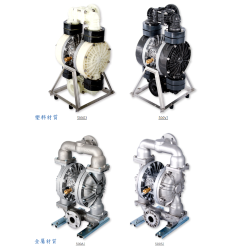
D500 Series
-
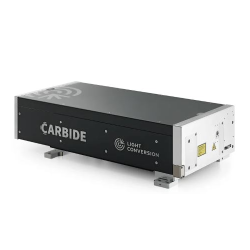
Femtosecond Laser
-
Femtosecond Laser
-
Functional Water Production and Recycling Equipment
-
Single Wafer Wet Process Equipment
-

Batch Type Wet Station Bench
-

Wafer Support System (for TBDB)