SEMILAB TAIWAN CO. LTD.
Area: 電子生產製造設備
Booth No: N220
Website: https://semilab.com/
Exhibitor Profile
SEMILAB delivers advanced metrology solutions for semiconductor, More‑than‑Moore, solar, and display applications. Our 45 product lines and 300+ tools support full R&D‑to‑production workflows, covering electrical, optical , thin‑film characterization, and automation from manual stations to full fab‑level integration.
Brands
SEMILAB TAIWAN CO. LTD.
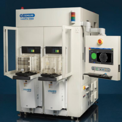
Exhibit Products
-
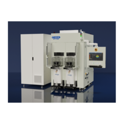
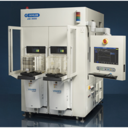
Advanced 3D Surface & Profile Metrology
-
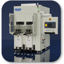
Wafer / carrier substrate edge profile measurement system (E-Shape)
-
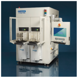
PSI 3000 Polarized Stress Imaging System
-
Raman Metrology for Stress and Crystalline Quality Control in Semiconductor Materials
-
MICROSPOT SPECTROSCOPIC ELLIPSOMETER (uSE)
-
300mm Spectral Photoluminescence system
-
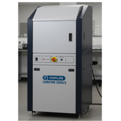
Contactless Resistivity Mapping Tool for 300 mm Semi‑insulating Wafers
-
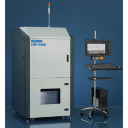
Spreading Resistance Profiling System with Integrated I‑V Measurement Capability
-
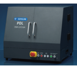
CARRIER-RESOLVED PHOTO & PARALLEL DIPOLE LINE HALL MEASUREMENT SYSTEM (PDL)
-
MicroLED functional inspection system based on photoluminescence imaging
Exhibitor Press Release
- Semilab introduces new, comprehensive metrology solution for microLED functional inspection 2026-02-27
- Semilab Launches New R&D Website to Highlight Material & Life Science Metrology Portfolio 2026-02-27
- Defect Inspection in the Early Stages of III-V Device Manufacturing 2026-02-27
Exhibitors you may be interested in
-
LIKUAN OPTO TECH INC.
-
G-LONG INTERNATIONAL TECHNOLOGY LTD.
-
MICROTEK INTERNATIONAL INC.
-

KAO LU ENTERPRISE CO., LTD.
-
HSIN CHENG YAO TECHNOLOGY CO., LTD.
-
HONG YANG LASER SERVICE CO., LTD.
-
IVORIST INTERNATIONAL CO., LTD.
-
IGUS TAIWAN COMPANY LIMITED
-
ONSET ELECTRO-OPTICS CO., LTD.
-

TECHPLASMA TECHNOLOGY CO., LTD.
-
CONVEYOR TRANSMISSION SYS CO., LTD.
-
TAIWAN SUPERCRITICAL TECHNOLOGY CO., LTD.
-
SCIENTECH CORPORATION
-
PHYSIK INSTRUMENTE (PI) TAIWAN LTD.
-
HONG I INSTRUMENTS CO., LTD.
-
RADIATION TECHNOLOGY CO., LTD.
-
TITAN ELECTRO-OPTICS CO., LTD.
-
SINOM CORPORATION
-
METAL INDUSTRIES RESEARCH & DEVELOPMENT CENTRE
-
HESHENG HARDWARE CO., LTD.
-
CHAN CHAO INTERNATIONAL CO., LTD.
-
GREAT CHAIN CHEMICAL LTD.
-
CHIEF SI INC.
-
CHEN BOM TRADING CO., LTD.
-
BAY UNION ABRASIVE TECHNOLOGY CO., LTD.
-
JIDIEN CO., LTD.
Highest Rated
-
HIWIN MIKROSYSTEM CORP.
-
GALLANT PRECISION MACHINING CO., LTD.
-

FAVITE INC.
-
TA LIANG TECHNOLOGY CO., LTD.
-
KINIK COMPANY LTD.
-
NANO-TREND TECHNOLOGY CO., LTD.
-
JOEN LIH MACHINERY CO., LTD.
-
BAY UNION ABRASIVE TECHNOLOGY CO., LTD.
-
METAL INDUSTRIES RESEARCH & DEVELOPMENT CENTRE
-

INDUSTRIAL ESTATE AUTHORITY OF THAILAND (I-EA-T)
-
UTECHZONE CO., LTD.
-
SYMTEK AUTOMATION ASIA CO., LTD.
-
MICRAFT SYSTEM PLUS CO., LTD.
-
HERMES-EPITEK CORP.
-
MOEA INNOVATION TECH HUB
-

C SUN MFG. LTD.
-
MARKETECH INTERNATIONAL CORP.
-
GROUP UP INDUSTRIAL CO., LTD.
-

ACM RESEARCH., INC.
-
HONOUR GLOW TRADING CO., LTD.
-
CONTREL TECHNOLOGY CO., LTD.
-
HESHENG HARDWARE CO., LTD.
-
NASCITECH INC.
-
WG TECH (GUANGDONG) INDUSTRIAL GROUP CO., LTD.
-
MICRO-EPSILON TAIWAN CO., LTD.
-

MANZ TAIWAN LIMITED
-
CPSYSTEM
-
TAIWAN SUPERCRITICAL TECHNOLOGY CO., LTD.
-
HEIDENHAIN CO., LTD.(TAIWAN)
-
CHROMA ATE INC.