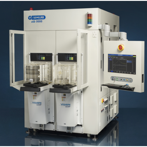
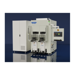
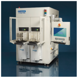
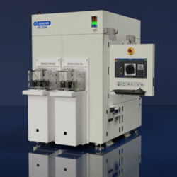
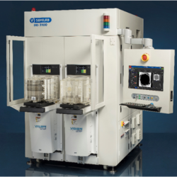
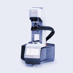
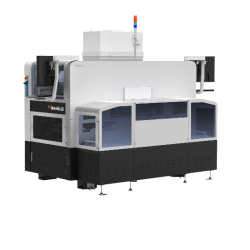
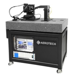
MICROSPOT SPECTROSCOPIC ELLIPSOMETER (uSE)
Model: uSE 3000
Category: Semiconductor Package Equipment
Exhibitor: SEMILAB TAIWAN CO. LTD.
Booth No: N220
Characteristic
SEMILAB SE Series – Accelerating Precision for Advanced IC Packaging
The SEMILAB SE Series brings industry‑leading ellipsometry technology to the fast‑evolving world of advanced IC packaging. Designed to meet the demands of multi‑layer dielectric stacks, RDL processes, hybrid bonding interfaces, and thin‑film metal layers, the SE Series enables manufacturers to monitor complex structures with unmatched accuracy and stability. With more than 30 years of ellipsometry expertise, Semilab provides an extensive materials library, powerful optical models, and proven process know‑how—ensuring reliable metrology performance from R&D to high‑volume manufacturing.
Why SE Series for Advanced Packaging?
Engineered for complexity: Ideal for PI/PBO stacks, low‑k dielectrics, UBM layers, micro‑bump structures, and hybrid bonding surface preparation.
Superior sensitivity: Detects subtle variations in thickness, refractive index, film uniformity, and surface conditions that directly influence device yield.
Ready for modern fabs: High‑throughput architecture, strong repeatability, and seamless automation make it ideal for production‑level process control.
Comprehensive materials support: Backed by a mature optical database and application expertise built through three decades of ellipsometry innovation.
Whether for wafer‑level or panel‑level packaging, the SEMILAB SE Series empowers engineers to control critical steps, ensure material integrity, and accelerate the path toward next‑generation performance.
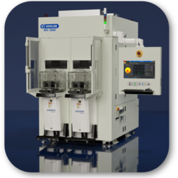
Other Products
-
Advanced 3D Surface & Profile Metrology
-
Wafer / carrier substrate edge profile measurement system (E-Shape)
-
PSI 3000 Polarized Stress Imaging System
-
Raman Metrology for Stress and Crystalline Quality Control in Semiconductor Materials
-
300mm Spectral Photoluminescence system
-
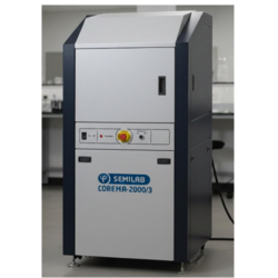
Contactless Resistivity Mapping Tool for 300 mm Semi‑insulating Wafers
-
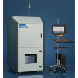
Spreading Resistance Profiling System with Integrated I‑V Measurement Capability
-
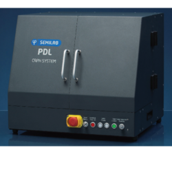
CARRIER-RESOLVED PHOTO & PARALLEL DIPOLE LINE HALL MEASUREMENT SYSTEM (PDL)
-
MicroLED functional inspection system based on photoluminescence imaging
Products you may be interested in
-
Silicone Rubber
-
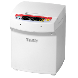
THINKY MIXER
-

Ultra nanoindentation tester
-
Electronic Vacuum Regulator (-100~600kPa)
-
Semiconductor Packaging Mold
-
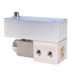
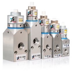
Enclosed Proportional Flow Control Valve
-
YAYATECH Post-Dicing IR Inspection Equipment
-
MCR Series (Modular Compact Rheometer)
-
Quantum Diamond Magnetic imaging microscope
-
Single Wafer Wet Process Equipment
-
Ultra nanoindentation tester
-
AOI Sorter
-
Glass Wafer Thickness Measurement System
-
Pactech POST-DICING IR INSPECTION
-
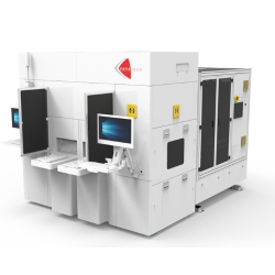
ZEISS 3D X-Ray Microscope
-
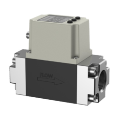
Stepper-Controlled Proportional Valve 0~5000L/min
-
Digital Flow Sensor For water
-
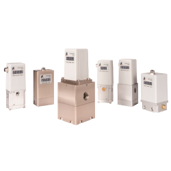
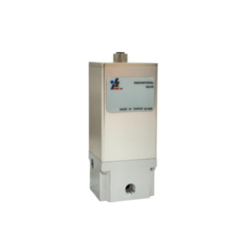
Electronic Proportional Pressure Regulator
-
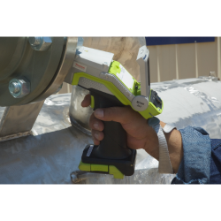
Thermo Niton XL5 Plus Handheld XRF Analyzer
-
AvantaGO L6
-
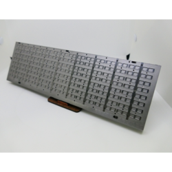
Spring Probe Socket
-
Differential Scanning Calorimeter - Julia DSC
-
Advanced Batch Type Baking Equipment
-
Data Enabler of the AI Era: Understanding CPO Co-Packaged Optics and PICAlign
-
Polyester film
Highest Rated Products
-
Copper Clad Laminate Thickness Measurement
-

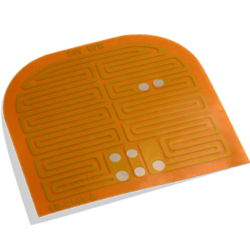
Patented Organic Chemical–Coated SiO₂ Far-Infrared Heat-Dissipating Particles
-
Glass-Wafer Wet bench system
-
Coater/Developer
-
UV Hybrid Dual-Cure Epoxy Adhesive
-
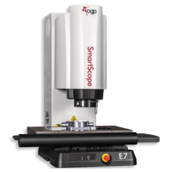
OGP E7 Fully Automatic Measurement System
-
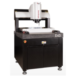
OGP E45 Fully Automatic Measurement System
-
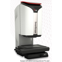
OGP M7 Fully 3D and Multisensor Capable BenchTop Dimensional Measurement System
-
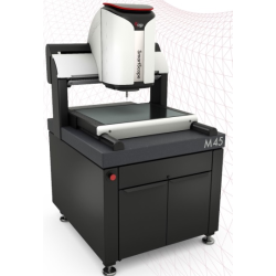
OGP M45 Fully 3D and Multisensor Capable BenchTop Dimensional Measurement System
-
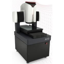
OGP M50 Fully 3D and Multisensor Capable BenchTop Dimensional Measurement System
-
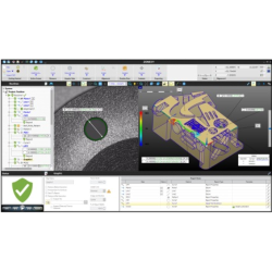
OGP ZONE3 Metrology Software
-
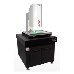
OGP SNAP350 Large Field Of View Video Measuring System
-
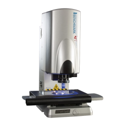
Benchmark250 Advanced Optical Metrology System
-
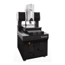
Summit 600 Advanced Optical Metrology System
-
Polyester film
-
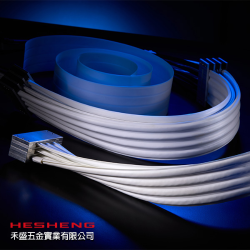
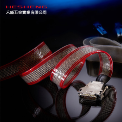
PTFE Cables for Semiconductor Applications
-
Servo motor connector
-
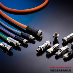
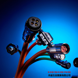
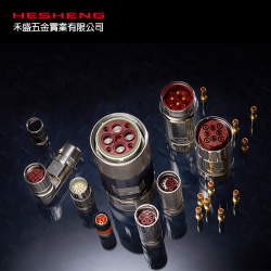
Circular Connector
-
Customized Cables
-
INTERCONTEC CONNECTOR
-
Polyimide film
-
Silicone Rubber
-
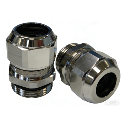
Cable glands nickel-plated brass
-
Casters、Leveling Feet
-
Wire Beam Processing Design And Manufacturing
-
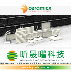
Ceramicx Infrared Heating Systems
-
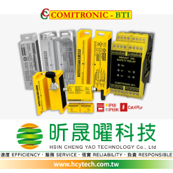
COMITRONIC-BTI Safety Switch And Safety Sensor
-
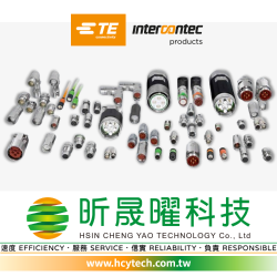
INTERCONTEC Connectors
-
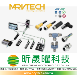
MARVTECH Circular Connectors
-
TE M8/M12/M16/M23/M36 Connector System