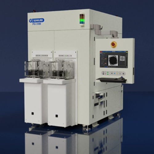
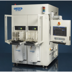
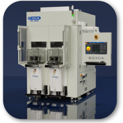
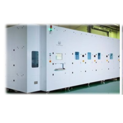
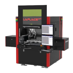
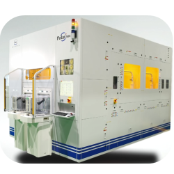
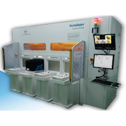
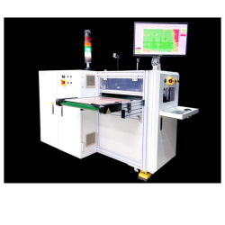
PSI 3000 Polarized Stress Imaging System
Model: PSI 3000
Category: Semiconductor Package Equipment
Exhibitor: SEMILAB TAIWAN CO. LTD.
Booth No: N220
Characteristic
The PSI product line from Semilab is engineered for deployment in high‑throughput, fully automated semiconductor fabs. These systems specialize in the detection, quantification, and visualization of crystal defects arising from mechanical stress within various substrate materials, including silicon wafers, silicon slugs, and glass components.
Leveraging polarized optical techniques, the PSI systems enable highly sensitive stress‑induced defect analysis by mapping birefringence patterns and stress‑related optical variations across the full wafer surface. This capability allows users to identify slip lines, dislocations, grain boundary disturbances, stress gradients, and other mechanically induced crystallographic anomalies with high spatial resolution.
Designed for 200 mm and 300 mm wafer manufacturing environments, the PSI platform supports fast automated wafer handling, stable measurement repeatability, and advanced image‑processing algorithms optimized for inline process control. These features make the PSI product line a critical tool for monitoring mechanical integrity during wafer manufacturing, post‑processing, and device integration steps.
Other Products
-
Advanced 3D Surface & Profile Metrology
-
Wafer / carrier substrate edge profile measurement system (E-Shape)
-
Raman Metrology for Stress and Crystalline Quality Control in Semiconductor Materials
-
MICROSPOT SPECTROSCOPIC ELLIPSOMETER (uSE)
-
300mm Spectral Photoluminescence system
-
Contactless Resistivity Mapping Tool for 300 mm Semi‑insulating Wafers
-
Spreading Resistance Profiling System with Integrated I‑V Measurement Capability
-
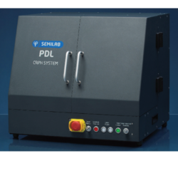
CARRIER-RESOLVED PHOTO & PARALLEL DIPOLE LINE HALL MEASUREMENT SYSTEM (PDL)
-
MicroLED functional inspection system based on photoluminescence imaging
Products you may be interested in
-
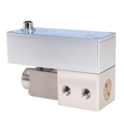
Electronic Vacuum Regulator (-100~600kPa)
-
Ultra nanoindentation tester
-
Batch Type Wet Station Bench
-
AOI Sorter
-
Wafer Support System (for TBDB)
-
Quantum Diamond Magnetic imaging microscope
-
OHMPLUS GT-S Middle Electronic Box (MEB)
-

Glass Wafer AOI Defect Inspection System
-
Stepper-Controlled Proportional Valve 0~5000L/min
-
Spring Probe Socket
-
Pactech POST-DICING IR INSPECTION
-

Ultra nanoindentation tester
-
Single Wafer Wet Process Equipment
-
AvantaGO L6
-

1-5 Acres Detached Factory
-
YAYATECH Post-Dicing IR Inspection Equipment
-
Differential Scanning Calorimeter - Julia DSC
-
Advanced Batch Type Baking Equipment
-
Wafer form EMC trimming Eqipment
-
Data Enabler of the AI Era: Understanding CPO Co-Packaged Optics and PICAlign
-
High Pressure Electronic Pressure Regulator(0~100bar)
-
Digital Flow Sensor For water
-
ZEISS 3D X-Ray Microscope
-
Polyester film
-
Enclosed Proportional Flow Control Valve
Highest Rated Products
-
Copper Clad Laminate Thickness Measurement
-

Patented Organic Chemical–Coated SiO₂ Far-Infrared Heat-Dissipating Particles
-
Glass-Wafer Wet bench system
-
Coater/Developer
-
UV Hybrid Dual-Cure Epoxy Adhesive
-
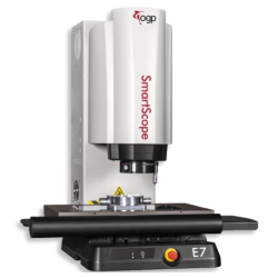
OGP E7 Fully Automatic Measurement System
-
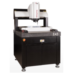
OGP E45 Fully Automatic Measurement System
-
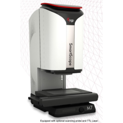
OGP M7 Fully 3D and Multisensor Capable BenchTop Dimensional Measurement System
-
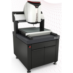
OGP M45 Fully 3D and Multisensor Capable BenchTop Dimensional Measurement System
-
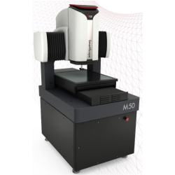
OGP M50 Fully 3D and Multisensor Capable BenchTop Dimensional Measurement System
-
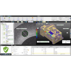
OGP ZONE3 Metrology Software
-
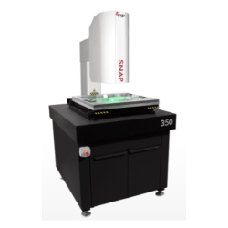
OGP SNAP350 Large Field Of View Video Measuring System
-
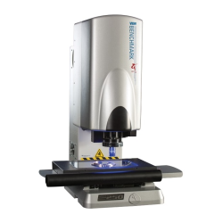
Benchmark250 Advanced Optical Metrology System
-
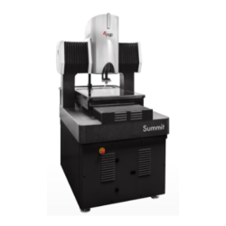
Summit 600 Advanced Optical Metrology System
-
Polyester film
-
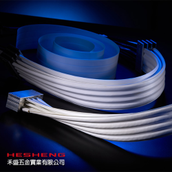
PTFE Cables for Semiconductor Applications
-
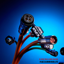
Servo motor connector
-
Circular Connector
-
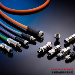
Customized Cables
-
INTERCONTEC CONNECTOR
-
Polyimide film
-
Silicone Rubber
-
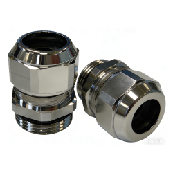
Cable glands nickel-plated brass
-
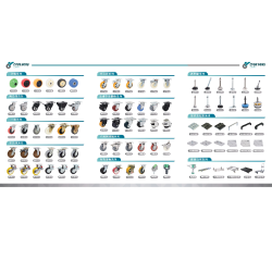
Casters、Leveling Feet
-
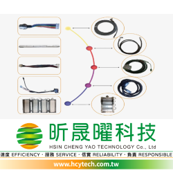
Wire Beam Processing Design And Manufacturing
-
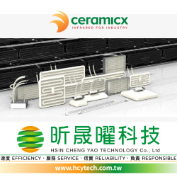
Ceramicx Infrared Heating Systems
-
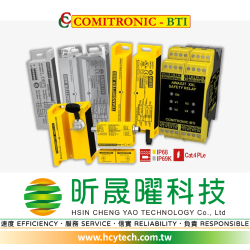
COMITRONIC-BTI Safety Switch And Safety Sensor
-
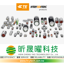
INTERCONTEC Connectors
-
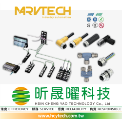
MARVTECH Circular Connectors
-
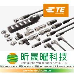
TE M8/M12/M16/M23/M36 Connector System