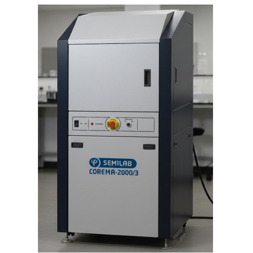
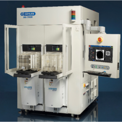
Contactless Resistivity Mapping Tool for 300 mm Semi‑insulating Wafers
Model: COREMA-2000/3
Category: Compound Semiconductor Equipment
Exhibitor: SEMILAB TAIWAN CO. LTD.
Booth No: N220
Characteristic
Semilab’s COREMA product line, built on a highly sensitive contactless capacitance‑based technique, is designed to meet the demands of routine production monitoring and quality assurance for semi‑insulating compound semiconductor wafers. The system provides high‑precision resistivity characterization across an exceptionally wide resistivity range, enabling reliable assessment of material uniformity, electrical behavior, and substrate quality without requiring any electrical contacts or surface preparation.
- Semi‑insulating GaAs/InP/SiC: Incoming inspection; post‑epitaxy background and defect indication.
- III–V materials: Within‑wafer/lot‑to‑lot uniformity and drift monitoring.
- RF/opto substrates: Screening for power amplifiers, photodetectors, microwave/mmWave devices.
- Process development & excursion analysis: Quantifying impacts from furnace, anneal, cleaning, and growth parameters.
Other Products
-
Advanced 3D Surface & Profile Metrology
-
Wafer / carrier substrate edge profile measurement system (E-Shape)
-
PSI 3000 Polarized Stress Imaging System
-
Raman Metrology for Stress and Crystalline Quality Control in Semiconductor Materials
-
MICROSPOT SPECTROSCOPIC ELLIPSOMETER (uSE)
-
300mm Spectral Photoluminescence system
-
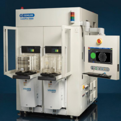
Spreading Resistance Profiling System with Integrated I‑V Measurement Capability
-
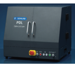
CARRIER-RESOLVED PHOTO & PARALLEL DIPOLE LINE HALL MEASUREMENT SYSTEM (PDL)
-
MicroLED functional inspection system based on photoluminescence imaging
Products you may be interested in
-
Ultra Low Expansion Glass ceramics CLEARCERAMTM-Z
-
Thermo Niton™ XL3t GOLDD+ Handheld XRF anaylzer
-
Glass Melting Factory Taiwan Ohara Optical Material Co.,Ltd
-
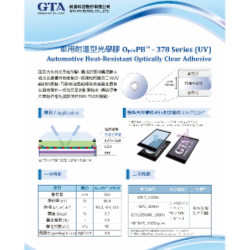
Automotive Heat-Resistant Optically Clear Adhesive - 378 Series (UV)
-
Compound Semiconductor Etching System
-
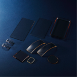
6-inch/8-inch SiC 4H N-Type/ S.I.-Type Substrate
-
Shock Resistant and High Hardness Clear Glass Ceramics NANOCERAM
-
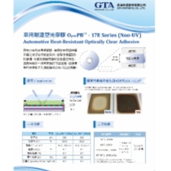
Automotive Heat-Resistant Optically Clear Adhesive - 17E Series (Non-UV)
-
VAD-process Synthetic Fused Silica SK-1300 Series
-
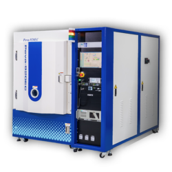
E-Beam Evaporator
-
Refractive index nd2.0 high transmittance optical glass S-LAH99W
-
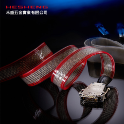
PTFE Cables for Semiconductor Applications
-
ADVANTEC pH test paper
-
DMA 5002+ Xsample 5200 Density Measurement Systems
-
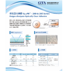
Outgas-dissipate Optically Clear Adhesive - 28D & 285 Series
-
ADVANTEC Membrane Filter
-
Thermo Scientific RadEye Multi-Purpose Survey Meters
-
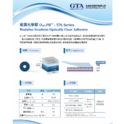
Modulus-Gradient Optically Clear Adhesive - 576 Series
-
Coater/Developer
-
Ultrapyc series Gas Pycnometers
-
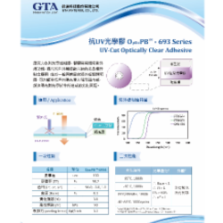
UV-Cut Optically Clear Adhesive - 693 Series
-
Patented Organic Chemical–Coated SiO₂ Far-Infrared Heat-Dissipating Particles
-
High-Modulus Optically Clear Adhesive - 83B Series
-
SCIL Nanoimprint Solutions High Precision Nanoimprint Solutions
Highest Rated Products
-
Copper Clad Laminate Thickness Measurement
-
Patented Organic Chemical–Coated SiO₂ Far-Infrared Heat-Dissipating Particles
-
Glass-Wafer Wet bench system
-
Coater/Developer
-
UV Hybrid Dual-Cure Epoxy Adhesive
-
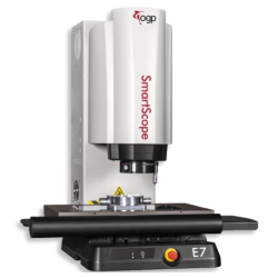
OGP E7 Fully Automatic Measurement System
-
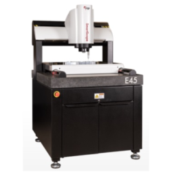
OGP E45 Fully Automatic Measurement System
-
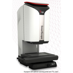
OGP M7 Fully 3D and Multisensor Capable BenchTop Dimensional Measurement System
-
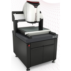
OGP M45 Fully 3D and Multisensor Capable BenchTop Dimensional Measurement System
-
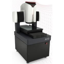
OGP M50 Fully 3D and Multisensor Capable BenchTop Dimensional Measurement System
-
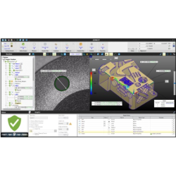
OGP ZONE3 Metrology Software
-
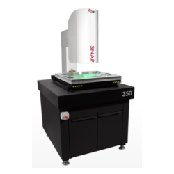
OGP SNAP350 Large Field Of View Video Measuring System
-
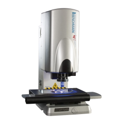
Benchmark250 Advanced Optical Metrology System
-
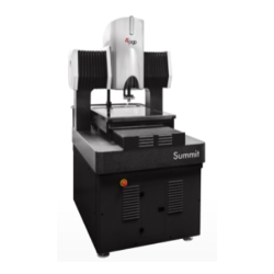
Summit 600 Advanced Optical Metrology System
-
Polyester film
-
PTFE Cables for Semiconductor Applications
-
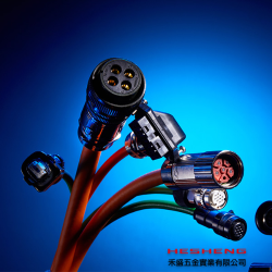
Servo motor connector
-
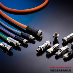
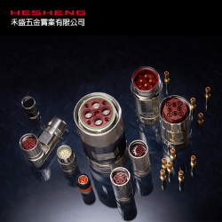
Circular Connector
-
Customized Cables
-
INTERCONTEC CONNECTOR
-
Polyimide film
-
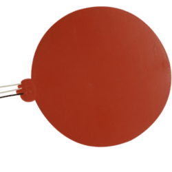
Silicone Rubber
-
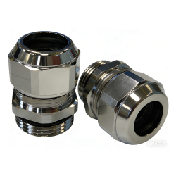
Cable glands nickel-plated brass
-
Casters、Leveling Feet
-
Wire Beam Processing Design And Manufacturing
-
Ceramicx Infrared Heating Systems
-
COMITRONIC-BTI Safety Switch And Safety Sensor
-
INTERCONTEC Connectors
-
MARVTECH Circular Connectors
-
TE M8/M12/M16/M23/M36 Connector System